Monday, September 19, 2011

Oiling Apparatus

In my last post I ended stating that I should probably do another test on a copper board to test my depth of cut (so I know how wide my isolation paths will be). I did that test. I either broke the tip or severely dulled it because I can't get any clean lines with it now. This is a 5 dollar Dremel conical cutting bit (HSS). I figured it was worth a try. I decided to order a proper 0.015" end mill in carbide. I also ordered a 1/6" bit. I've got an 1/8" and 3/8" so that gives me a good amount of flexibility.

I also ordered all the electronic components for the 2 PCB boards. While I'm waiting for all the stuff to come in, I thought I'd take care of a maintenance problem. The Y lead screw and ways are super easy to oil. The X is very difficult. It's all underneath the table so hard to see, plus gravity pulls the oil down so you have to get it above the part to be oiled. So I made a simple oiling tool. I picked up a cheap "rear view extension" mirror for a car and liberated it from the mounting system:


I also got some tubing with 1/6" ID:


This is a "variety pack" - it's got 2 items in it both with 1/16" ID but different ODs. Anyway. I made a "wand" out of 14ga house wire. I put some heat-shrink tube around the end to hold the tube to the wand. Another piece of heat-shrink at the other end of the tube made for a nice adaptor for the oil can. Here's a pic of it all on the workbench:


I'm a capable photographer, but I'm finding many of my shop pics are looking rather crappy. Like many, this has some focus problems. You can see the mirror under the X/Y table showing the X lead screw and ways. I'm holding the wand in the lower left. That's the oil can that says "oil" on it. I hold the oil in one hand, wand in the other, then gain a boatload of appreciation for my dental hygienist that can do fine manipulations in a mirror. I dumped way too much oil on the system the first time, but better than too little.

I also started work on my halloween costume. Here's the goal:


Wednesday, September 7, 2011

Scaling Problem Fixed

In my last post I said my circuit board path test resulted in an engraving that was 80% of the size it was supposed to be. That number didn't ring any bells at the time. Later that evening I was brushing my teeth and thought, "What's 72/90?" I grabbed my phone (my Sharp scientific calculator died years ago) and ran the numbers. The answer? 0.8!

So where did I get 72 and 90? I remembered reading somewhere recently that Inkscape (the SVG drawing program I'm processing the design with) works in "pixels" as its base unit of length. "Pixel" is short for "picture element". It's the smallest dot the computer can make on the screen. Which means it's pretty arbitrary. The actual length of a line 150 pixels long depends on the size of the monitor and the resolution the display is set to. Anyway, what I read said Inkscape assumes 90 pixels per inch.

Years ago when I worked in graphic design, monitors were smaller and video displays were lower resolution. Back then, 72dpi, dots per inch or really pixels per inch was the convention. So there're the 2 numbers that popped in my head. I wondered if there was some error in the software. Obviously not mine since I did a Java-only path that measures out correctly.

The GCode plug-in I'm using in Inkscape is written in Python which I know a little about. I couldn't find any factors for scaling hard-coded into the exporter. The plug-in asks Inkscape for the conversion factor. I set my document to inches and sure enough it returns 90 like the documentation said it would. I simply hard-coded 72 as the scale factor, exported the GCode again and my host software reported the proper extents.

I ran the program and got this:


It's pretty hard to measure such a thing as this. Using my dial caliper and magnifying glass I took a couple of rough measurements. The PCB design software says the traces are "thin" or 0.016". I expanded the path to use as much room as possible (two adjacent circles nicely come together at a tangent) and the traces seem to be closer to 20 mils. The small pads for the DB-25 I measured somewhere around 60 mils. According to Inkscape the pads are... 60 mils. That's pretty cool.

I drilled a hole with my 1/32" drill bit, the smallest I have. There isn't much room around it. I definitely need a smaller bit. I might reshape the pads, make them rectangles, to give me more room to solder.

So it looks promising. My goal was to determine if I could isolate the paths and still leave enough copper to solder to and looks clear that will work. Really I should do another test on some real copper to check the isolation using the depth-of-cut I used on this test.

Ok, I just ran downstairs and did a test on a scrap perf board. The depth I used on the red piece was 10 mils. That didn't cut all the way through. I dropped down 5 more and it cut clean. According to a quick geometry check in QCad, the difference in width from a 10 mil deep cut to a 15 mil deep cut is 3.3 mils. I don't think that's significant, so I'm still feeling positive.

On more thing. You might notice the pad circles are not real, well, circular. I'm sure this is the effect of the backlash I'm totally ignoring at this point. I'll address that another day.

Monday, September 5, 2011

Circuit Board Design

I spent a fair amount of time working in Fritzing on the circuit board designs. One is for the box that holds the manual controls (the control panel), the other goes in the box with the stepper driver control board. I'm exporting the PCB design as an "etchable" SVG. Here is a first draft of the control panel:


Along the top is the DB-25 connector. The holes are a little over 0.100" apart but as you can see I have to get a trace in between each one. The traces in this illustration are 0.016" wide. I'm using a conical cutting bit and I don't know how deep I'll have to cut to isolate. Once I figure that out I'll be able to figure out how wide the cutting path will be. My concern is that I'll be cutting a path that's wider than the space between the traces and the traces will be too thin. Worse is that the pads will be too thin and I'll drill it all away.

The etchable design then goes through some manipulation to expand the elements to account for the width of the cutting bit. Then I export to GCode using a plug-in in Inkscape.

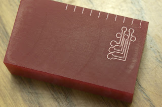
I mixed up a pot of plaster of paris and made a brick to do some practice cuts on. I don't have any pictures of it because it's not very impressive. I made up a test design that incorporates both the size and spacing of the DB-25 pads and traces plus standard 0.100" pads. I squared up a piece of cured polyurethane resin and cut the test path:


I arranged the path to make the pads and traces as large as possible, i.e., the path around the pads is more or less coincidental with the path along the traces between the pads. While is looks like it will isolate ok, it seems quite tight. The smallest drill bit I have is 1/32" which will probably create a hole around 0.050". I think that will wipe out the small holes on the DB-25 connector. Not good.

The three larger pads at the lower left are standard-size holes on 0.100" spacing. Or are they? I held up a standard header pin thingy against the three holes and they don't add up. ("Cat don't want to eat mice, wants dog to massacre him...") I wrote a quick program entirely in Java to cut the lines across the top at 0.100" intervals and they line up just right with the header. So something is wrong with my tool chain.

The good news it that the path is too small, so when it's fixed the pads and traces will hopefully be big enough to accommodate the 1/32" drill. I added a feature to the host software to calculate the extents of the mill movement, the minimum and maximum positions on each axis. Here's a screenshot of the SVG design. The page is sized to the path.


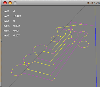
As you can see, the path area is 0.34 by 0.53. Here's the host software with the extents displayed:


The min X and Y are 0, the max are 0.273 by -0.425. It's 80% of actual size. I'll have a look at the plug-in for generating the GCode. Maybe there's some unit conversion error.

All in all, I'm not happy with the GCode generating tools. I've got 2 plug-ins for Inkscape. One is very minimal, the other is quite complex and neither has much in the way of documentation. So I may end up writing my own SVG reader to generate paths in the Java model.